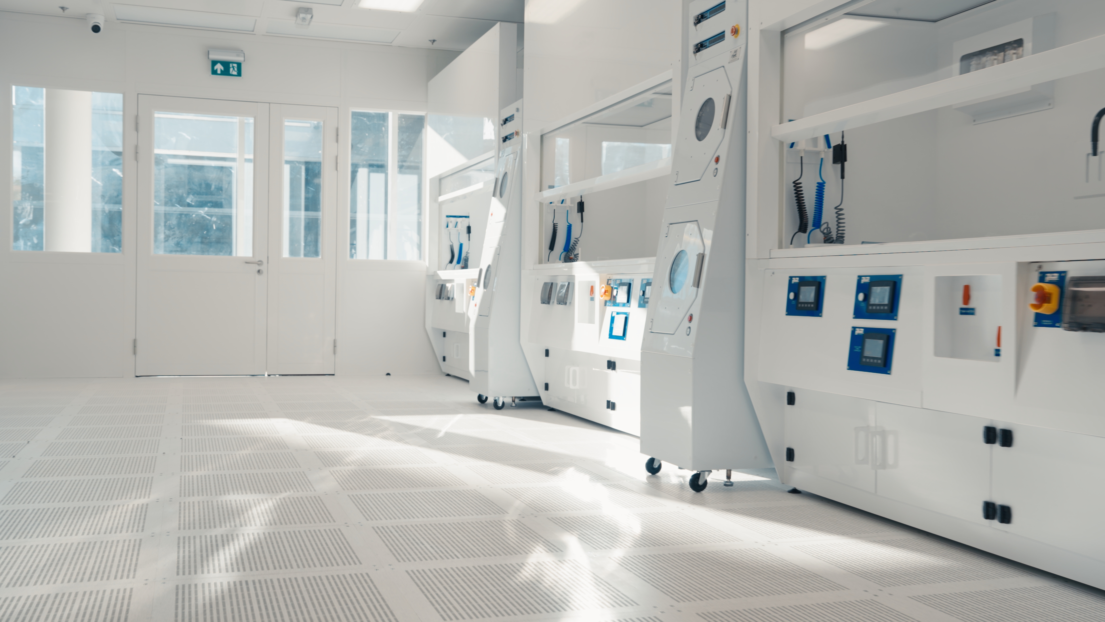
Electron Beam Lithography
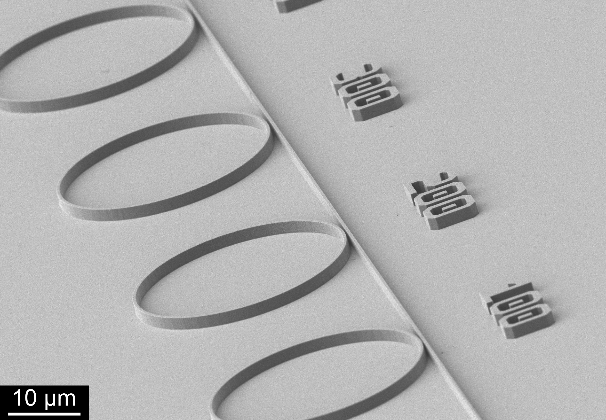
Direct write 100kV electron-beam lithography exposures for ultra-high resolution pattern definition of nanoscale features. Compatible sample sizes ranging from small tiles (<10 mm) up to 200 mm diameter wafers. Established EBL processes include positive (PMMA, ZEP520), negative (HSQ, AZnLOF) and lift-off (PMMA/MMA) resists to meet a range of applications. This includes, where appropriate, hybrid optical-electron beam exposures to decrease the patterning times of larger wafers. Processes have been established on a range of material systems including non-conductive samples using current spreading layers (thin metal PVD or conductive polymers).
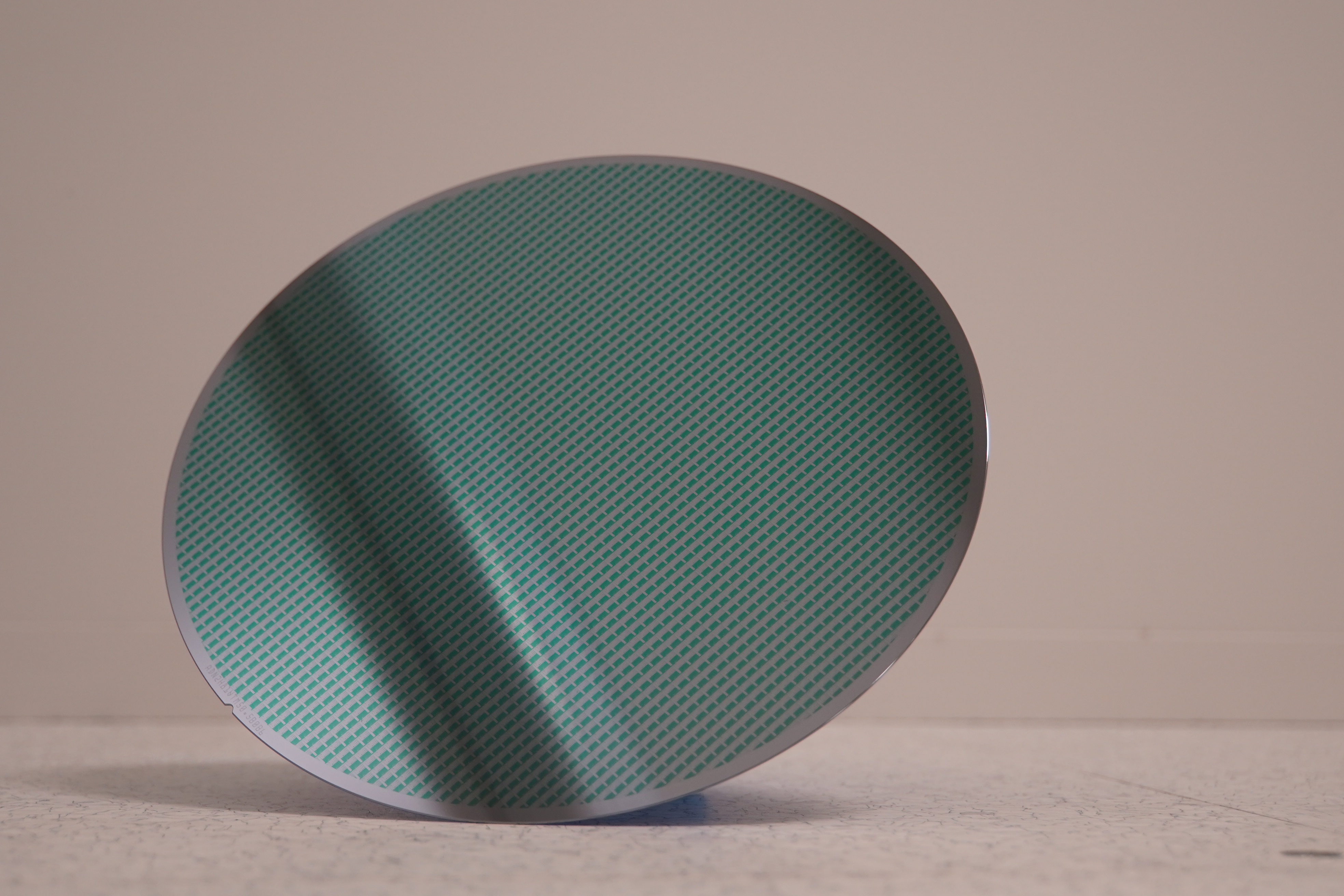
Optical Lithography
Mask aligners with i line, g line, and broadband UV wavelengths and maskless photolithography tools with i line exposure along with spinners, developer tools and a SUSS HMX 9 mask cleaner housed in an ISO class 5 dedicated bay. Established processes with mask aligners and maskless photolithography tools that are compatible from small tiles up to 200 mm diameter wafers with sub micron features with a range of positive, negative, and bi layer photoresists to meet the requirements of our applications. Processes have been established on a Silicon, GaAS, InP, SiC, GaN, Diamond, Quartz, Dielectric and metal surfaces. Hybrid processes have been established between optical-electron beam exposures.
Plasma Etch and Deposition
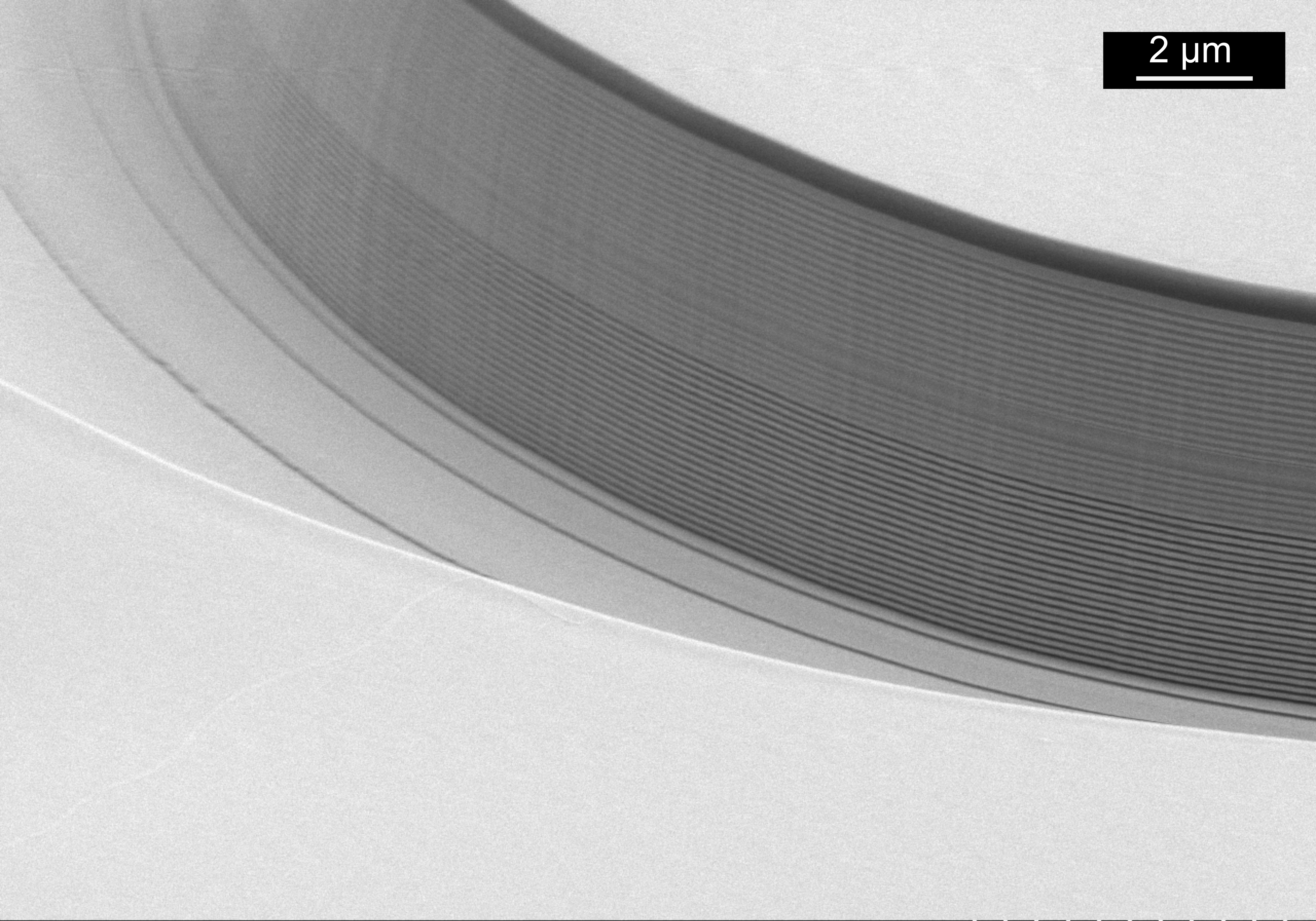
Inductively coupled plasma reactive ion etching systems with capability to etch a wide range of films including III-V materials, dielectrics and metals. The high-density reactive species at low pressures achieve high etch rates with low selectivity, excellent uniformity with clean smooth vertical profiles and etch surfaces. Laser endpoint detection used for precise targeting. Systems can be configured to etch small pieces up to 200mm wafers.
Thin Film Deposition
Thin films of metals and dielectrics can be deposited using a physical vapour deposition technique including electron beam evaporation, thermal evaporation or magnetron sputtering. High quality dielectrics can also be deposited using plasma enhanced chemical vapour deposition (PECVD) or atomic layer deposition (ALD) techniques. Multiple deposition systems calibrated to ensure backup redundancy with established processes for low resistance III-V ohmic contacts and passivation layers.
Thermal Processing
High-temperature processes including annealing, rapid thermal processing (RTP), and diffusion used to activate dopants and improve film properties.
Metrology
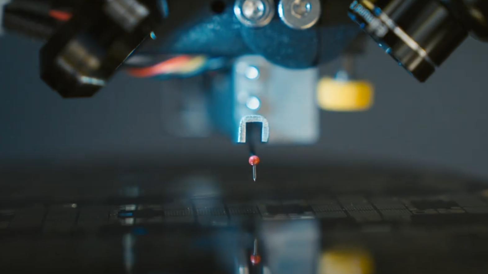
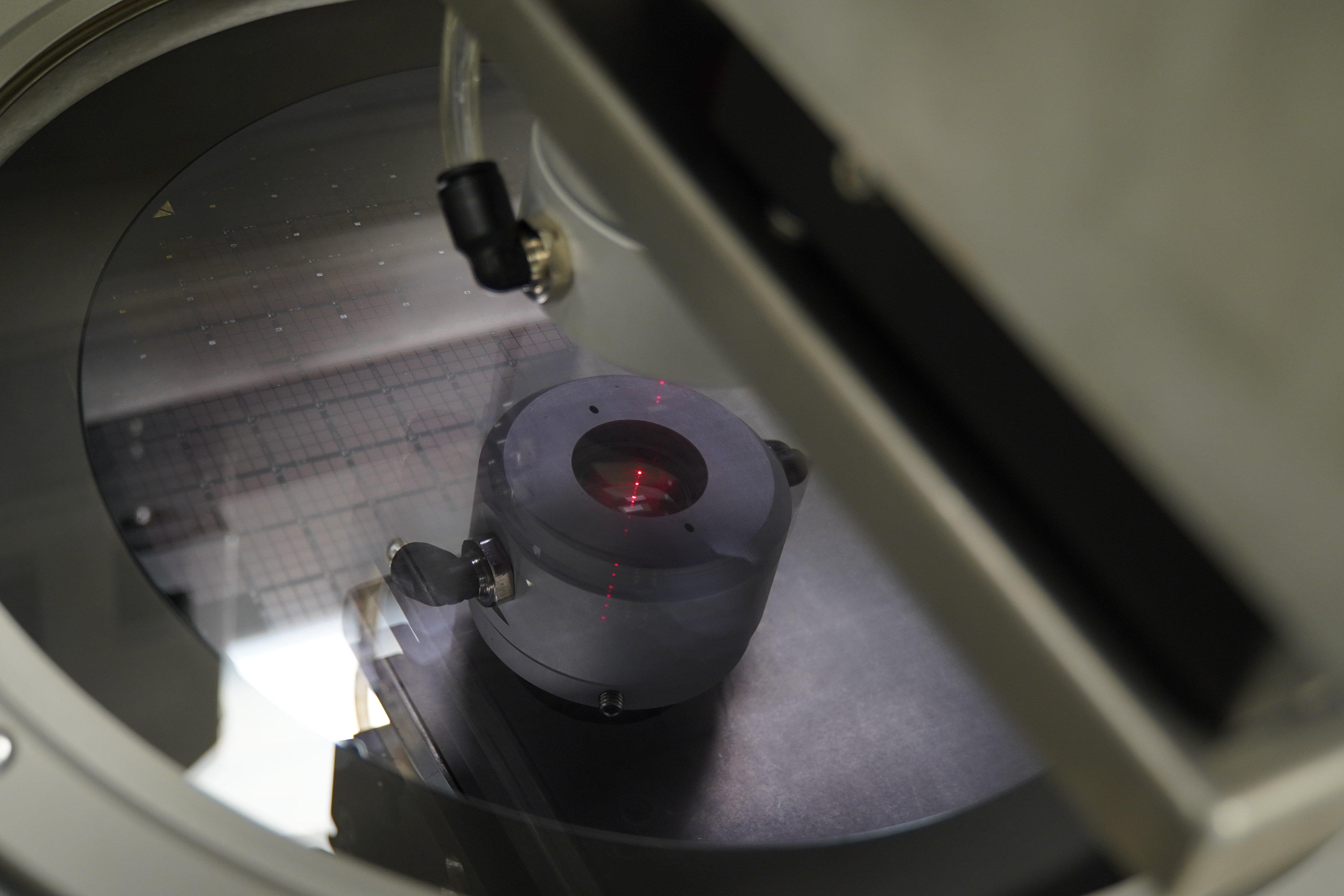
Dimensional, electrical and optical measurements (SEM, ellipsometry, profilometry, probe testing) for process control and device verification.
Oxidation
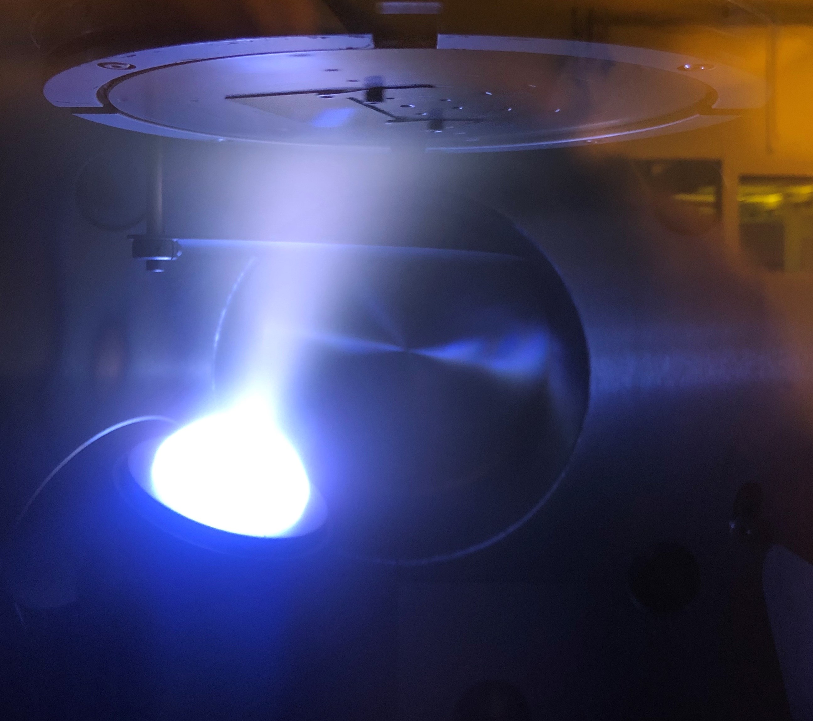
Used for the controlled oxidation of AlGaAs/AlAs layers in the fabrication of Vertical Cavity Surface Emitting Lasers (VCSELs) and other devices with similar material systems. Capable of running small tiles (<10 mm) up to 200 mm diameter wafers with established processes in place to correct wafer-bow for improved oxidation uniformity. In-situ monitoring of oxidation extents using an infra-red microscope for maximum process control. Full wafer mapping of oxidised structures is also available.
Wet Chemistry
Dedicated wet chemistry bay with established processes to cater from small tiles up to 200mm wafers. These processes include HF acid based etches, Piranha based etches along with other standard silicon and compound semiconductor etches.